

Share with your CTO
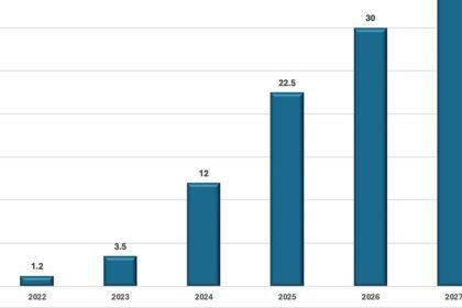
Qualcomm is making a direct run at Nvidia’s data center dominance with a new chip architecture called high-bandwidth compute, built around stacking low-power DRAM directly on top of the logic die rather than beside it. The company claims this delivers up to six times higher bandwidth per watt compared to conventional HBM-based designs. Under the Dragonfly brand, Qualcomm is targeting $5 billion in data center revenue by fiscal 2027 and $15 billion by 2029, with the first HBC-based product shipping as the AI250 rack in 2027.
What this means for your business
Your AI infrastructure procurement cycle and the timeline at which you’re locked into it will determine whether this matters to you now or two years from now. Organizations that are signing multi-year GPU commitments today are effectively betting against architectural alternatives arriving at commercial scale by 2026. Those with more flexible infrastructure strategies, or those still in early design phases for inference-heavy workloads, have room to hold and watch whether Qualcomm actually ships at the claimed efficiency numbers.
The honest read on Qualcomm’s claim is that the physics are sound but the execution risk is substantial. Stacked memory, where DRAM sits directly on the compute die connected through vertical channels called through-silicon vias, is not a new idea. SK Hynix and Samsung have been working on near-memory compute approaches for years without reaching mass production. Qualcomm’s argument is that its packaging expertise from decades of smartphone chip design gives it a commercialization path the memory vendors lacked. That’s a plausible differentiator, not a guaranteed one, and the 2027 ship date gives the company roughly two years to prove it before Nvidia’s next generation resets the benchmark.
The inference angle is where this cuts deepest for enterprise buyers. Training workloads, the ones that built Nvidia’s moat, are concentrated among hyperscalers with their own negotiating power. Inference, which is the ongoing cost of running AI models at scale inside your products and operations, is where most enterprise AI spend is heading and where memory bandwidth per watt is the actual cost driver. If Qualcomm delivers even half of the claimed efficiency gain at production scale, it reshapes the cost-per-query math that currently makes large-scale AI deployment prohibitively expensive for most companies outside the Fortune 100.
The decision this reframes isn’t whether to buy Qualcomm today. It’s whether your current infrastructure vendor agreements have enough flexibility to incorporate a credible second source for inference acceleration by 2028. Single-vendor lock-in at the chip layer has always carried strategic risk; it carries more now that the architectural assumptions underpinning that layer are genuinely in play. If your next data center contract has no off-ramp for alternative accelerator architectures, that’s worth scrutinizing before the ink dries.
Concept deep-dive: High-bandwidth memory (HBM)
HBM is the specialized memory type that sits beside AI processors in today’s data center chips, connected through a silicon interposer, which acts like a dense circuit board bridge. It was designed to feed data to GPUs fast enough to keep them busy. The limitation is physical distance: data still has to travel laterally between memory and compute, consuming energy and creating latency. Qualcomm’s stacked approach collapses that gap vertically, which is the architectural bet the entire HBC roadmap rides on.
Based on reporting from Qualcomm takes on Nvidia with new AI chip architecture | Taiwan News, originally published 2026-07-01 06:00:00.