


Share with your CTO
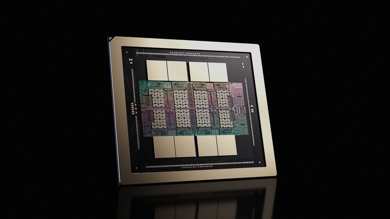
NVIDIA’s Rubin Ultra accelerator, positioned as the 2027 performance flagship, may ship with less on-package memory than the chip it replaces. A TrendForce report from August 4 shows NVIDIA is now evaluating four HBM configurations for Rubin Ultra, including an 8-Hi HBM4 option that SemiAnalysis says yields 192 gigabytes per GPU. The current Vera Rubin already ships with 288 gigabytes. That’s not a slip in ambition; it’s a supply chain rewriting the Rubin Ultra specification before NVIDIA has finalized it.
What this means for your business
If your 2027 AI infrastructure sizing was anchored to the original Rubin Ultra spec, the ground has already shifted at least twice. This isn’t a single engineering revision. TrendForce documents three separate memory subsystem compressions across the Rubin platform in six months: server RDIMM reductions, a halving of SOCAMM capacity on Vera CPU modules from 192 to 96 gigabytes, and now HBM itself under review. The pattern isn’t bad luck; it’s a structural DRAM shortage writing chip specs in real time, and organizations running 2027 planning cycles on published roadmaps are working from numbers that supply constraints have already invalidated.
The HBM4 versus HBM4E distinction matters beyond capacity. HBM4E (the “Enhanced” variant, running the same wide memory interface at nearly double the data rate) was supposed to push Rubin Ultra’s per-pin I/O speed to 14-16 gigabits per second. A fallback to HBM4 caps that at 11-12 Gbps, a 25-35 percent throughput gap that maps directly to token output on large language model inference workloads where memory bandwidth is the binding constraint. A CTO who has committed rack counts, cluster network design, or cost-per-token targets around the HBM4E spec is holding a position that hasn’t been confirmed.
The deeper problem is structural, not cyclical. HBM requires three to four times the wafer area of standard DRAM to produce the same number of gigabytes. New fab capacity from Samsung’s Pyeongtaek P5 megafab and SK Hynix’s M15X facility doesn’t reach meaningful output before mid-2027 at the earliest and 2028 for the rest. NVIDIA’s $500 billion-plus partnership with SK Group, announced in July, exists precisely because priority allocation at scale requires multi-year commitments that most buyers can’t make. The organizations without that kind of leverage are the ones whose planning assumptions are most exposed.
Build three parallel infrastructure models now, before production commitments lock: one at 384 gigabytes per GPU (original spec, still possible if HBM4E qualifies), one at 288 gigabytes (parity with current Rubin), one at 192 gigabytes (the SemiAnalysis mainstream scenario). Rack counts, interconnect bandwidth, and per-token economics differ materially across those three cases. The procurement decision to revisit isn’t whether to buy Rubin Ultra; it’s whether the workload sizing and cluster architecture your team defended in a 2025 planning cycle still holds against a chip that may underperform its predecessor on memory.
Concept deep-dive: HBM stack height
High Bandwidth Memory is built by stacking individual DRAM dies vertically and connecting them with through-silicon vias, microscopic copper pillars drilled through each layer. Think of it as a multi-story parking structure where each floor is a memory die. A 12-Hi stack has 12 floors; an 8-Hi stack has 8. Each die must be ground down to about 50 micrometers, roughly the width of a human hair, before stacking. Fewer layers means lower capacity per chip but higher manufacturing yield, which is why supply pressure pushes vendors toward shorter stacks even when it means shipping less memory.
Based on reporting from NVIDIA Rubin Ultra AI Chip May Deliver Less HBM Than Rubin, Forcing Procurement Replanning, originally published 2026-08-05 11:03:00.